Contact Us
Email:info@opticsledlens.com
Tel: + 86-755-29059599
Fax: + 86-755-29056599
Zip code: 518109

News
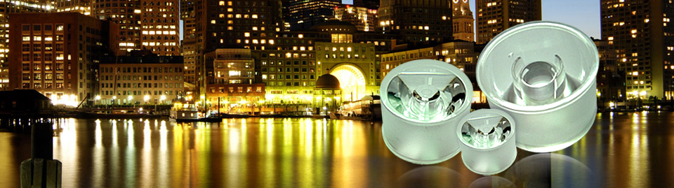
Your current location:Home > News > Company newsHigh-voltage(AC) LED lens(Ⅰ)
Views: Date:2012/8/8

1. COBLED packaging methods can be divided into the LENS-TYPE and REFLECTOR-TYPE, which the lens of the molding can be molded or lens bonding molding; reflective chip is more rubber mixing point plastic package molding.
Given the comprehensive consideration of the insulation, pressure, heat, and heat, the ceramic substrate to become one of the important materials for chip-adhesive technology. Its technology can be divided into a thick-film technology , LTCC technology , thin film technology and other ways. Thick film technology and low-temperature co-fired technology, screen printing technology with high temperature sintering process, easy to produce rough lines, imprecise, and the contraction ratio of more sophisticated high-power LED products for the line, or require accurate eutectic or flip-chip technology, the LED products, the thick film and low temperature co-fired ceramic substrate, apparently increasingly unable to meet the requirements.
To this end, the high thermal coefficient of film radiating ceramic substrate using sputtering, electrical / chemical deposition and photolithography process is made with metal line is accurate, the stability of the material system characteristics, applicable to high power, small size, high brightness LED the development trend is the solution to the eutectic / flip-chip packaging technology, the stringent requirements of the metal line resolution and accuracy of the ceramic substrate. . When the LED chip to the ceramic as a carrier board, the bottleneck of the LED module heat transferred to the system board, the heat transmitted by the LED chip to the heat sink and the atmosphere, with the gradual improvement of the LED chip features, materials gradually from FR4 to a metal core printed circuit board (MCPCB), but with the demand for high-power LED progress, the thermal coefficient of the material in the MCPCB (2 ~ 4W/MK) can not be used for higher power products, ceramic circuit board (CERAMIC CIRCUIT BOARD) demand for the increasing popularity, to ensure the stability of the material stability of LED products in the high-power operation of the light fades, the trend of the ceramic as a heat and metal wiring substrate has become increasingly clear. Ceramic materials currently cost more than MCPCB, therefore, if the characteristics of ceramic high-heat coefficient, saves material use area to reduce production costs, to become one of the important indicator of the ceramic LED development. In recent years, the integration of a polycrystalline ceramic materials COB design package and system lines gradually being of great importance to the package and system vendors.
COB, in the electronics manufacturing industry is not a fresh, refers directly to the bare wafer adhesive in the circuit board and wire / wire soldered directly to the gold-plated line on the PCB, is also commonly known as wire (WIRE BONDING), through the technology of plastic closures, effective package of steps in the IC manufacturing process transferred to the circuit board assembly directly. In addition, in the LED industry, more and more stress due to modern technology products light weight and high portability, directly in order to save system board space for the many LED chip design in the demand for high-power LED system, we developed the chip adhesive The system board of
COB technology.The advantages of the COB is: cost-effective, simple circuit design, system board space savings, but also the existence of the chip integrated brightness, color temperature to reconcile the threshold of the technology and systems integration. 25W of LED, for example, the traditional high-power 25W LED light source, with 25 1W LED chip package into 25 LED components and COB packaging is 25 1W LED chip is packaged in a single chip, requiring The second optical lens from the 25 reduced to one to help narrow light area, reduce materials, and system cost savings. In addition, high power COB packaging only a single high power LED to replace the more stars 1 watt (or more) LED package to promote the product volume is thinner and lighter. Currently on the market, production COB products still use MCPCB substrate-based, however, the MCPCB still a lot of heat and light area is too large to be solved, ceramic COB substrate has the following advantages: (1) thin film technology, to ensure more accurate line (2) large amount of lower cost. high plasticity, do the design according to different needs.
The development of ceramic MCOB / COB is to simplify the system board of a trend, practical lighting, brightness, heat, and cost control, are important factors.